


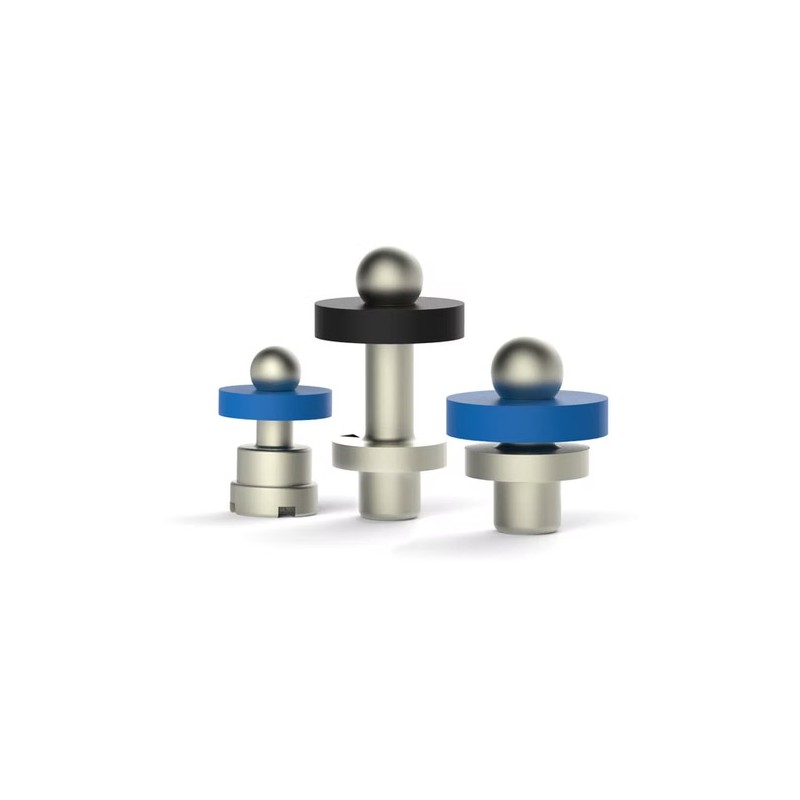
Solderball Pin Autosplice
Solderball Pin Autosplice is a product in the field of solderball pin / SMT interconnect pin / board-to-board connector / PCB stacking terminal / high-current PCB connection, developed and supplied by Autosplice to electronics, telecommunications, industrial equipment, medical device, power module businesses, and electronic circuit board manufacturers.
The product is used to create electrical and mechanical connections between a main board and a sub-board or between multiple PCBs arranged in parallel. Solderball Pin is suitable for electronic modules requiring optimized board space, reduced connector size, multiple boards arranged in a stacked configuration, or combining signal and power transmission within the same assembly.
Autosplice does not apply a fixed Solderball Pin configuration for all designs. The chosen solution is based on connection type, terminal size, solder ball diameter, height between PCBs, number of pins, mounting position, current, voltage, pad structure, SMT reflow process, mechanical requirements, production volume, and the specific usage conditions of each customer.
1. Key Features of the Product
Solderball Pin combines a conductive metal terminal with a precisely formed solder ball at the PCB contact point.
The product can be supplied in tape-and-reel format for use with automated pick-and-place machines in SMT lines.
After placement on the PCB, the solder ball melts during the reflow process to create an electrical and mechanical connection between the terminal and the board.
Terminal length can be selected to determine the spacing between the main board and the sub-board.
The product is available in through-hole, SMT, SMT-to-SMT configurations and versions for high-current applications.
Terminals can use straight pin, tapered pin, or multi-step structures depending on the assembly method.
The solder ball can help compensate for coplanarity deviations between PCBs during the reflow process.
Each pin can be placed at the required position on the board, reducing the need for a large connector or rerouting traces to a fixed area.
The product can be used for signal, power connections, or a combination of both within the same PCB assembly.
Connection quality depends on terminal configuration, pad size, amount of solder material, board coplanarity, reflow temperature, and assembly control process.
2. What Needs Does the Product Meet?
Autosplice Solderball Pin is suitable for:
- Multi-stacked or parallel PCB assemblies.
- Power modules and power converters.
- Telecommunications equipment and network systems.
- Industrial controllers.
- High-density electronic devices.
- Medical devices and measurement systems.
- Products requiring board-to-board connections.
- Designs requiring reduced connector footprint.
- Automated SMT assembly lines.
- Applications requiring signal or high-current transmission.
For signal designs, customers can prioritize small-sized terminals and multiple placement positions on the board.
For power modules or high-current applications, it is necessary to select terminal size, number of pins, and pad structure appropriate for the electrical load and operating temperature.
3. Consultation and Supply Process
The process may include:
- Receiving drawings and connection requirements.
- Defining main board and sub-board structure.
- Selecting through-hole, SMT, or SMT-to-SMT type.
- Determining the stacking height between PCBs.
- Selecting pin diameter and solder ball size.
- Determining the number and position of terminals.
- Evaluating current, voltage, and thermal requirements.
- Checking pad size and reflow process.
- Confirming samples and specifications.
- Providing samples or proceeding with mass production.
For new designs, customers should provide PCB assembly drawings, board dimensions, pin layout diagrams, current, voltage, desired height, and anticipated SMT process.
For high-volume orders, it is necessary to provide estimated production volume, pick-and-place machine type, tape-and-reel specifications, inspection standards, and delivery schedule.
3.1. Solderball Pin Selection Criteria
The product is selected based on:
- Connection type between PCBs.
- Number of boards in the assembly.
- Spacing between the main board and sub-board.
- Terminal diameter and length.
- Solder ball size.
- Number and position of connection pins.
- Current and voltage at each terminal.
- Pad size on the PCB.
- Board thickness and material.
- Coplanarity of the PCB assembly.
- Reflow process and temperature.
- Mechanical durability requirements.
- Production volume and packaging method.
Signal transmission applications should prioritize compact pin arrangement and spacing suitable for circuit density.
Power transmission applications require attention to terminal cross-section, number of pins, heat dissipation capability, and current limits of the entire assembly.
3.2. Information Customers Need to Provide
Customers should provide:
- 2D drawings or 3D data of the PCB assembly.
- Dimensions of the main board and sub-board.
- Layout diagram of connection pins.
- Connection type: through-hole, SMT, or SMT-to-SMT.
- Spacing between PCBs.
- Number of pins required.
- Current and voltage at each position.
- Pad size or PCB hole.
- Board thickness.
- Flatness and tolerance requirements.
- SMT reflow process parameters.
- Estimated production volume.
- Packaging specifications.
- Inspection standards and required delivery time.
The more complete the information, the more accurately product selection, sample development, quotation, and supply planning will align with actual needs.
3.3. Inspection and Storage
Before assembly, it is necessary to check the correct product code, terminal size, solder ball diameter, pin length, component quantity, and tape-and-reel packaging condition.
The pad surface on the PCB must be clean, flat, and compatible with the solder ball size. Solder paste, reflow temperature, and heating time must be set according to the board material and product configuration.
After the reflow process, it is necessary to check terminal position, solder joint shape, uniformity, pin misalignment, insufficient solder, solder bridging, or abnormal deformation.
Visual inspection, AOI, X-ray, resistance testing, continuity testing, and functional testing can be used depending on product requirements.
Solderball Pins should be stored in intact packaging, in a dry, clean environment, and protected from dust, high humidity, or chemicals that could affect the solderable surface.
4. Benefits for Customers and Businesses
The product helps create connections between multiple PCBs without the need for large-sized connectors.
The individual pin design allows for direct placement of terminals at the required signal or power transmission points.
The ability to select pin length helps customers control the stacking height between boards.
Tape-and-reel packaging supports integration of the product into existing SMT lines and pick-and-place machines.
Solder balls can help compensate for coplanarity deviations between PCBs, contributing to stable connections during the reflow process.
For electronics manufacturers, the product facilitates modular design development, reduces PCB area, and offers flexibility in changing the number or position of connections.
For mass production businesses, standardized configurations can support control over process, quality, and assembly costs.
5. Highlights and Suitable Customers
Product highlights include:
- Main board to sub-board connection.
- Suitable for multi-stacked PCB assemblies.
- Combines metal terminals with precise solder balls.
- Compatible with SMT reflow processes.
- Supplied in tape-and-reel format.
- Suitable for pick-and-place machines.
- Available in through-hole, SMT, and SMT-to-SMT configurations.
- Versions for signal or high-current transmission.
- Supports PCB stacking height selection.
- Individual pins can be placed at required positions.
- Helps reduce connector footprint.
- Capable of compensating for coplanarity deviations.
- Suitable for modular designs.
- Configurations can be developed according to project requirements.
Autosplice Solderball Pin is suitable for PCB manufacturers, EMS companies, electronics, telecommunications, industrial equipment, power module, medical device companies, and customers requiring compact, automated, and flexible board-to-board connection solutions.
Autosplice supports customers from receiving drawings, selecting terminal type, determining solder ball size, stacking height, current carrying capacity, to providing samples and implementing production tailored to each PCB assembly.
Jigs / Construction machinery parts / Manufacturing facilities
CONTACT
Inquiry for the above productCompany Information

Press-fit terminal and pin header / Terminal, pin, and connector / Automated assembly equipment and solutions
Autosplice Electronics (Dongguan) Co., Ltd. designs, manufactures, and supplies terminals, pins, connectors, precision stamped parts, molded products, interconnect assemblies, and automated equipment ...